APVV-25-0467 / 2026–2029

Applied Research on an Athermal SiON Photonic Platform

How can an optical filter stay at the same wavelength as its chip warms up? AthermalGuide investigates materials and waveguide geometries that can suppress this shift.

Explore the research
AthermalGuide · APVV-25-0467

About the project

Planned project period
09/2026 – 08/2029

Project abstract

AthermalGuide targets applied research, design, and experimental validation of an athermal waveguide structure for photonic integrated circuits (PICs) based on silicon oxynitride (SiON) combined with a PMMA polymer cladding exhibiting a strongly negative thermo optic coefficient. The objective is to achieve a negative thermal dispersion of the effective refractive index that compensates both the thermal expansion of the silicon substrate and the positive thermo optic contributions of the waveguide and buffer layers, thereby enabling thermally stable operation of key photonic components.

The athermal stack will be engineered by tuning the SiON refractive index during PECVD, selecting layer thicknesses, and optimising waveguide geometry so that the target negative temperature coefficient of the effective index is reached. Preliminary results from the team indicate that a hybrid PMMA/SiON/SiO₂/Si configuration can limit the temperature dependent wavelength shift of AWG filters to below 0.718 pm °C⁻¹, representing a clear improvement over conventional dielectric platforms.

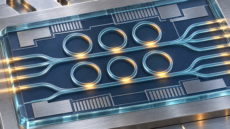
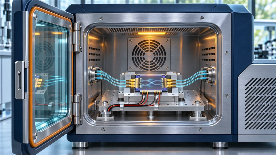
Within the project, spectral photonic elements—including ring resonators, unbalanced Mach–Zehnder interferometers, and AWG devices—will be designed and fabricated to quantify resonance shifts and phase variations across −40 °C to +80 °C. A dedicated temperature controlled measurement facility will be built and validated, employing dry nitrogen operation to ensure stable, condensation free characterisation of optical parameters.

The principal outcome will be a validated athermal waveguide platform accompanied by design rules and a Process Design Kit (PDK). This foundation will enable the design and fabrication of a broad class of temperature stable passive photonic components on silicon for telecommunications, sensing systems, and other domains where suppression of thermal effects is critical.

What is athermal photonics?

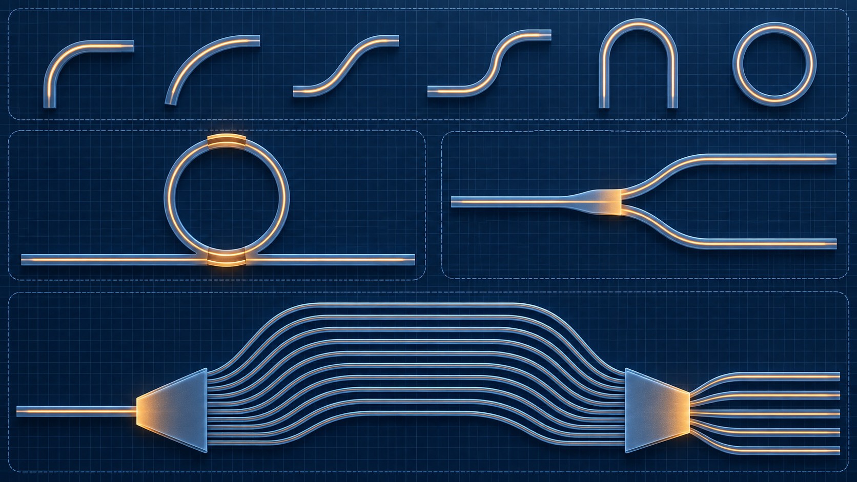
A waveguide carries light across a chip. A temperature change alters the material’s refractive index, shifting the wavelength transmitted by an optical filter. Athermal design combines material composition and waveguide geometry to minimise that shift.

Objectives and expected benefits

The team studies silicon oxynitride (SiON), designs passive photonic components and plans to test their stability from −40 °C to +80 °C. More stable filters could reduce the need for active heating or cooling in optical communications and sensing systems.

Research and project phases

WP-1

Materials

Deposit SiON layers and measure refractive index, optical loss and thermal response.

  • T1.1 Vary the N₂O/SiH₄ ratio, RF power, pressure and substrate temperature during PECVD.
  • T1.2 Characterise films by ellipsometry, AFM and SEM, measure spectral loss and extract the thermo-optic coefficient.
  • T1.3 Select two to three reference material stacks for device design.
  • T1.4 Test long-term stability and analyse hydrogen-related absorption.
WP-2

Circuit design

Simulate waveguides, resonators and filters, then prepare the first mask set.

  • T2.1 Model the temperature-dependent effective index, group index and thermal wavelength shift using FEM/FDTD.
  • T2.2 Design an athermal waveguide cross-section using thermo-optic compensation and dispersion engineering.
  • T2.3 Design AWGs, MZIs, ring resonators and delay lines and analyse their tolerances.
  • T2.4 Lay out the masks, design thermal test structures and run DRC/LVS checks.
  • T2.5 Submit the first tape-out and confirm acceptance.
WP-3

Measurement platform

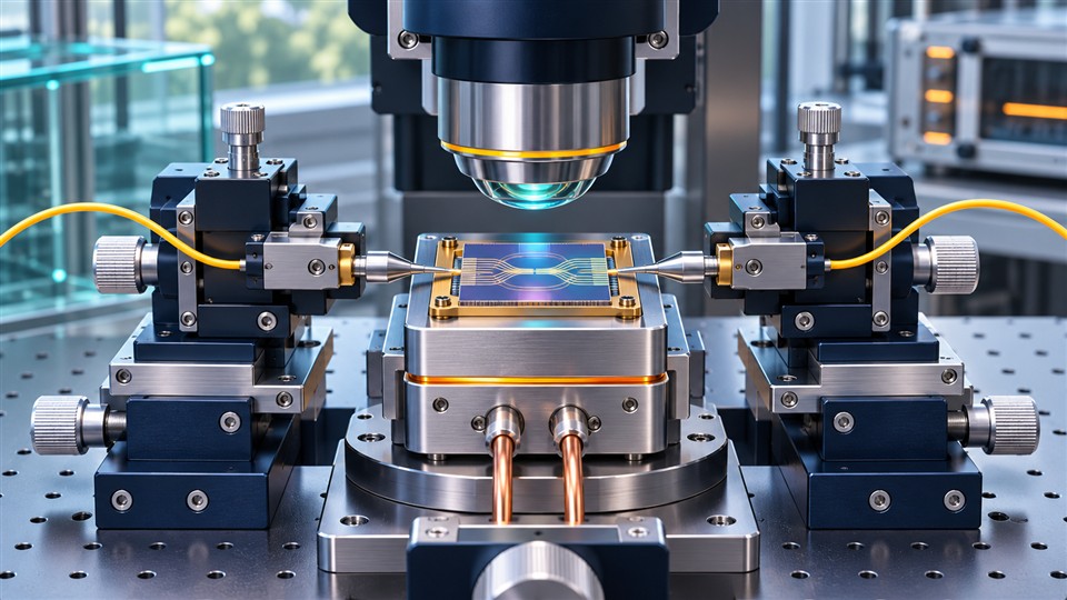
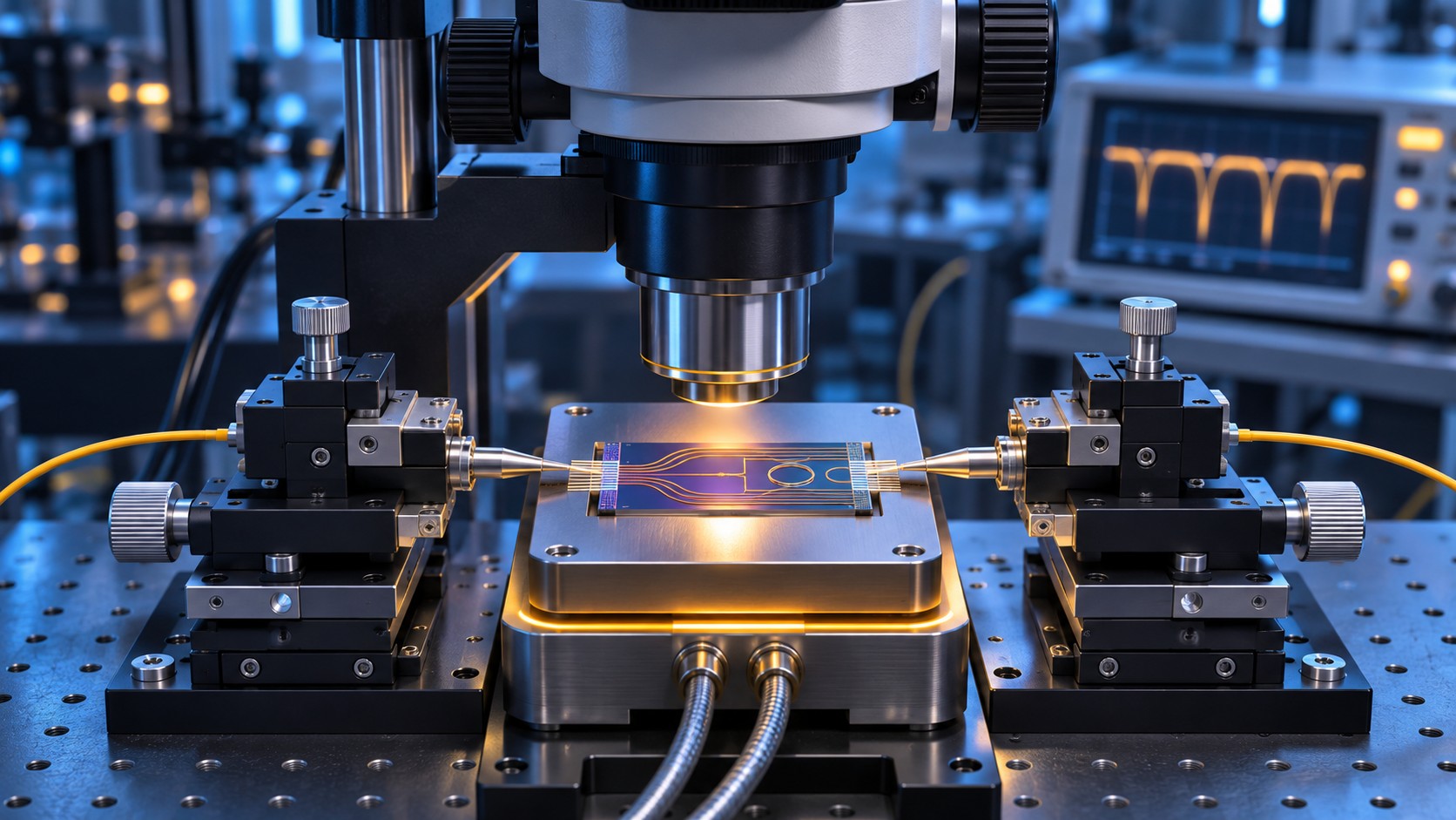
Develop a temperature-controlled platform with dry nitrogen for optical measurements.

  • T3.1 Design and model the thermal architecture of the platform.
  • T3.2 Design the mechanical and optomechanical assemblies.
  • T3.3 Integrate the electronics and control loops.
  • T3.4 Assemble, integrate and debug the platform.
  • T3.5 Validate thermal performance, calibrate the platform and prepare its operating protocol.
  • T3.6 Measure photonic circuit performance across temperatures.
WP-4

First fabrication run

Compare measurements from the first chips with the design models.

  • T4.1 Complete final checks on the first mask set and prepare for fabrication.
  • T4.2 Fabricate the first batch of chips.
  • T4.3 Characterise the fabricated chips.
  • T4.4 Perform initial validation and compare results with the design models.
WP-5

Design rules and PDK

Translate the findings into design rules, component libraries and documentation.

  • T5.1 Extract process parameters and design constraints.
  • T5.2 Define the PDK architecture and core libraries.
  • T5.3 Prepare verification decks and design rule checks.
  • T5.4 Prepare the technology transfer package.
WP-6

Second run and reliability

Validate revised designs through thermal cycling and long-term stability tests.

  • T6.1 Refine the design and prepare the second mask set.
  • T6.2 Fabricate the second batch of chips.
  • T6.3 Characterise the optical and thermal properties of the fabricated chips.
  • T6.4 Test reliability and long-term stability, including thermal cycling.

Results and publications

Results

Material data and models for SiON waveguide design

Open PDF

A calibrated test platform and photonic chip measurements

Open PDF

A process design kit (PDK) with a component library and design rules

Open PDF

Publications

Investigation of Chromatic Dispersion Properties of Athermal 100 GHz Cyclic AWG for Super PON

Jozef Chovan, Ignác Bugár, Anton Kuzma, Martin Tomaška · 2025 17th International Conference on Advanced Infocomm Technology · 2026

Open full PDF – Investigation of Chromatic Dispersion Properties of Athermal 100 GHz Cyclic AWG for Super PON

Calibration-Oriented Analysis of ITU-T Grid Alignment Limits in Athermal Cyclic Arrayed Waveguide Gratings

Jozef Chovan, Dana Seyringer, Anton Kuzma, Martin Tomáška, Ignác Bugár · Preprint · 2026

Open full PDF – Calibration-Oriented Analysis of ITU-T Grid Alignment Limits in Athermal Cyclic Arrayed Waveguide Gratings

Research team

Jozef Chovan

Principal investigator

He combines photonic chip design with experiments on fibre-to-chip coupling, automated assembly and the temperature response of optical circuits.

Soňa Kováčová

FEI work package lead

She specialises in thin-film lithography and fabrication. She examines the surface topography of fabricated structures using atomic force and scanning electron microscopy.

Ignác Bugár

Femtosecond spectroscopy

His research covers ultrashort optical pulses and microstructured fibres. He measures the thermo-optic coefficient and performs optical ellipsometry.

Daniel Figura

Microtechnology and fabrication

He works in the cleanroom, depositing films by PECVD and patterning them with optical lithography and ICP-RIE plasma etching.

Andrej Vincze

SIMS materials analysis

He uses secondary ion mass spectrometry to map surfaces and measure depth profiles in thin waveguide films, providing feedback for fabrication.

Miroslav Michalka

Electron microscopy

His background is in pulsed laser deposition of metal films. He examines waveguides and photonic devices using scanning electron microscopy.

Martin Ziman

Photonic modelling and design

He leads the modelling and design of athermal waveguides and devices. He develops compact models and parameterised cells and integrates fabrication data into the process design kit.

Jaroslav Kováč

Advanced spectroscopy

He characterises materials using high-resolution Raman spectroscopy and advanced atomic force microscopy techniques.

Daniel Haško

Surface characterisation

He examines materials and fabricated components using atomic force and 3D optical microscopy and evaluates the resulting surface measurements.

Martin Tomáška

Measurement platform and metrology

He brings experience in microwave electronics and optoelectronics to the design, implementation and certification of the WP-3 platform and its measurements.

Anton Kuzma

Numerical modelling and coordination

He models photonic and polymer structures using RCWA, FDTD and BPM, incorporates process data into the PDK and coordinates project activities at STU.

Ľuboš Podlucký

Dielectric films and optical metrology

He fabricates dielectric layers using PECVD, etching and photolithography and measures their optical properties by ellipsometry and refractometry.

Michal Hausner

Doctoral student

He implements and characterises electronic and optical systems for automating optical experiments.

Martin Feiler

Simulation and experimental electronics

He simulates the physical properties of proposed structures and builds electronic systems for optical experiments.

Financial and administrative project management

Lenka Balnova

Project financial manager

CVTISR

She prepares the project budget, provides financial documentation for procurement and prepares the financial section of the final project report. She follows institutional rules and the funding requirements of the project.

Nataša Učnová

Project financial manager

FEI STUBA

She prepares the project budget, provides financial documentation for procurement and prepares the financial section of the final project report. She follows institutional rules and the funding requirements of the project.

Project partners

CVTI SR

International Laser Centre · SCSTI

The centre specialises in laser processing, precision assembly and testing of photonic components. It coordinates the project and its public outreach. It leads the design of athermal waveguides and circuits, develops the platform for measuring their thermal response and leads work on the process design kit (PDK).

Team members

STU FEI

Institute of Electronics and Photonics · FEI STU in Bratislava

The institute deposits thin dielectric films and patterns photonic circuits using lithography and plasma etching. It leads the development and characterisation of SiON/SiO₂ layers and both chip fabrication runs. The team tests the fabricated devices against design models and evaluates their thermal stability and reliability.

Team members

News

Master’s thesis topics for the 2026/2027 academic year

The Institute of Electronics and Photonics at FEI STU is offering five master’s thesis topics. Open a topic to read its full description.

Automated Measurement of Spectral and Polarization Characteristics of Photonic Integrated Circuits

Basic information

Thesis type
Master’s thesis
Slovak title
Automatizované meranie spektrálnych a polarizačných charakteristík fotonických integrovaných obvodov
English title
Automated Measurement of Spectral and Polarization Characteristics of Photonic Integrated Circuits
Topic status
Approved by the study programme guarantor, prof. Ing. Ľubica Stuchlíková, PhD.
Supervisor
J. Chovan
Faculty
Faculty of Electrical Engineering and Information Technology
Responsible institute
Institute of Electronics and Photonics – FEI
Maximum number of students
1
Applications
Any number of students may apply until the available place has been filled by an approved applicant.
Academic year
2026/2027
Proposed by
Ing. Jozef Chovan, PhD.
Abstract
Photonic integrated circuits are important components of modern optical communication systems, particularly those that use wavelength-division multiplexing (WDM). Using these circuits in practice requires experimental measurements of their transmission characteristics, including spectral response, insertion loss, interchannel crosstalk and polarization-dependent loss (PDL). The student will learn how to measure the transmission characteristics of photonic integrated circuits and design software to automate PDL measurement and analysis. This will involve studying how integrated WDM components work, which instruments are used to test them and how their spectral characteristics are measured. The student will assemble and configure a test setup, measure the transmission spectra of selected WDM components and develop software to acquire and process the data needed to determine PDL as a function of wavelength. The thesis will deliver a working PDL measurement tool, validate it experimentally on selected photonic integrated circuits and evaluate the main transmission parameters of those circuits.
Modeling and Performance Analysis of Optical Communication Systems Incorporating Photonic Integrated Circuits

Basic information

Thesis type
Master’s thesis
Slovak title
Modelovanie a analýza prenosových vlastností optických komunikačných systémov s fotonickými integrovanými obvodmi
English title
Modeling and Performance Analysis of Optical Communication Systems Incorporating Photonic Integrated Circuits
Topic status
Approved by the study programme guarantor, prof. Ing. Ľubica Stuchlíková, PhD.
Supervisor
J. Chovan
Faculty
Faculty of Electrical Engineering and Information Technology
Responsible institute
Institute of Electronics and Photonics – FEI
Maximum number of students
1
Applications
Any number of students may apply until the available place has been filled by an approved applicant.
Academic year
2026/2027
Proposed by
Ing. Jozef Chovan, PhD.
Abstract
Photonic integrated circuits enable advanced optical signal processing and transmission in modern optical communication systems. Incorporating these circuits affects attenuation, interchannel crosstalk, dispersion and transmission error rates. Numerical modelling makes it possible to analyse these effects and optimise system parameters before building an experimental system. The student will learn to model and simulate optical communication systems in Synopsys OptSim and incorporate models of photonic integrated circuits designed with Keysight RSoft Photonic Device Tools. The work covers physical-layer modelling, models of individual components and methods for evaluating transmission performance. The student will build a simulation of a selected optical communication system, incorporate photonic circuit models based on their simulated transmission characteristics and analyse how the circuits affect optical signal transmission quality. Particular attention will be paid to how insertion loss, interchannel crosstalk, spectral response and dispersion in integrated photonic components affect overall system performance. The thesis will deliver a working system simulation that includes the photonic circuit models and an assessment of their impact on transmission performance. The results can inform the design and optimisation of optical communication systems incorporating advanced integrated photonic components.
Design and Modeling of Thermal and Dispersion Characteristics of Photonic Integrated Circuits

Basic information

Thesis type
Master’s thesis
Slovak title
Návrh a modelovanie teplotných a disperzných vlastností fotonických integrovaných obvodov
English title
Design and Modeling of Thermal and Dispersion Characteristics of Photonic Integrated Circuits
Topic status
Approved by the study programme guarantor, prof. Ing. Ľubica Stuchlíková, PhD.
Supervisor
J. Chovan
Faculty
Faculty of Electrical Engineering and Information Technology
Responsible institute
Institute of Electronics and Photonics – FEI
Maximum number of students
1
Applications
Any number of students may apply until the available place has been filled by an approved applicant.
Academic year
2026/2027
Proposed by
Ing. Jozef Chovan, PhD.
Abstract
Photonic integrated circuits are key components of modern optical communication and sensing systems. Their transmission characteristics depend on material properties, optical waveguide geometry, chromatic dispersion and temperature changes. Accurate modelling of these effects is essential for designing photonic circuits that achieve a specified spectral response and maintain it as temperature varies. The student will learn to design and numerically model photonic integrated circuits, with an emphasis on their thermal and dispersion characteristics. The work covers light propagation in integrated waveguides, numerical modelling methods and specialised photonic circuit design software. The student will design and optimise selected integrated photonic structures, such as optical waveguides, interferometers or waveguide multiplexers. This will involve modelling the effective refractive index as a function of wavelength and temperature, analysing material and waveguide dispersion, and evaluating how temperature changes affect the transmission spectra of the proposed circuits. The student will also investigate how material selection and waveguide geometry can reduce temperature sensitivity. The thesis will deliver numerical models and designs for selected photonic integrated circuits, together with an assessment of their thermal and dispersion characteristics. The results can support the development of temperature-stable photonic circuits within the AthermalGuide research project.
Development of an Automated Test Setup for Temperature-Dependent Characterization of Photonic Integrated Circuits

Basic information

Thesis type
Master’s thesis
Slovak title
Vývoj automatizovaného pracoviska na teplotnú charakterizáciu fotonických integrovaných obvodov
English title
Development of an Automated Test Setup for Temperature-Dependent Characterization of Photonic Integrated Circuits
Topic status
Approved by the study programme guarantor, prof. Ing. Ľubica Stuchlíková, PhD.
Supervisor
J. Chovan
Faculty
Faculty of Electrical Engineering and Information Technology
Responsible institute
Institute of Electronics and Photonics – FEI
Maximum number of students
1
Applications
Any number of students may apply until the available place has been filled by an approved applicant.
Academic year
2026/2027
Proposed by
Ing. Jozef Chovan, PhD.
Abstract
The thermal stability of transmission characteristics is an important consideration when using photonic integrated circuits in optical communication and sensing systems. Testing this stability requires a dedicated setup that provides precise temperature control, stable optical coupling and reproducible measurement conditions over a wide temperature range. The student will contribute to the development of an automated test setup for the thermal characterisation of photonic integrated circuits within the AthermalGuide research project. The work covers thermoelectric cooling, resistive heating, temperature measurement and control, and the experimental requirements for characterising integrated photonic structures. The student will design, build and integrate selected parts of a setup that regulates temperature from −40 °C to +80 °C. This will involve implementing automated temperature control, monitoring and logging measurement data, maintaining thermal stability and protecting the sample from condensation. The student will also address the mechanical layout needed to maintain stable optical coupling to the circuits under test. The thesis will deliver a working temperature-controlled experimental setup and an evaluation of the accuracy, stability and repeatability of its temperature control. The setup can then be used to measure how the transmission characteristics of photonic integrated circuits vary with temperature.
Development of an Automated System for Precise Rotational Alignment of Polarization-Maintaining Optical Fibers

Basic information

Thesis type
Master’s thesis
Slovak title
Vývoj automatizovaného systému na presné natáčanie polarizáciu udržujúcich optických vlákien
English title
Development of an Automated System for Precise Rotational Alignment of Polarization-Maintaining Optical Fibers
Topic status
Approved by the study programme guarantor, prof. Ing. Ľubica Stuchlíková, PhD.
Supervisor
J. Chovan
Faculty
Faculty of Electrical Engineering and Information Technology
Responsible institute
Institute of Electronics and Photonics – FEI
Maximum number of students
1
Applications
Any number of students may apply until the available place has been filled by an approved applicant.
Academic year
2026/2027
Proposed by
Ing. Jozef Chovan, PhD.
Abstract
Polarization-maintaining (PM) optical fibres are used in modern optical communication, sensing and photonic systems that must preserve the polarization state of transmitted light. When splicing these fibres or assembling them into fibre arrays, the polarization axes of the individual fibres must be precisely aligned. Automating this process can improve the accuracy, repeatability and efficiency of fibre array assembly. The student will contribute to the development of an automated experimental setup for precise rotational alignment of PM optical fibres within the NATOPAV research project. The work covers the structure and properties of PM fibres, optical imaging of their cross-sectional microstructure and methods for determining the angular orientation of their polarization axes. The student will design, build and experimentally validate selected parts of the setup, including a camera-based imaging system, a motorised fibre rotation mechanism and process control software. The student will integrate these components and optimise the procedure for automatically setting the desired rotation angle using image feedback. The thesis will deliver a working experimental system for automated rotation of PM fibres and an assessment of its accuracy and repeatability. The system can support further development of multi-fibre splicing and coupling techniques.

For enquiries, email the thesis supervisor, Jozef Chovan, PhD, at jozef.chovan@cvtisr.sk.

Support for Talented Students at FEI STU – paid OFDR research at €200 per month

FEI STU is offering paid student research in electrical engineering. The position pays €200 per month for up to 30 hours per month. The initial phase runs from 10 January to 10 July 2027. To express your interest, email the project supervisor at jozef.chovan@stuba.sk.

Project details

Project details

Experimental coherent OFDR system for characterising photonic circuits
Supervisor: Ing. Jozef Chovan, PhD., Institute of Electronics and Photonics, FEI STU in Bratislava.

Aim and expected outcome

You will design, build and test a coherent optical frequency-domain reflectometry (OFDR) system to locate reflections inside optical circuits. You will build your own reference Mach–Zehnder interferometer (k-clock MZI), integrate the instruments and write the measurement software in Python.

You will investigate whether the system can measure photonic integrated circuits up to 20 cm long over a total measurement range of approximately 3.2 m, including the fibre leads. The target spatial resolution is 100 µm or better. You will determine the resolution experimentally.

The setup includes an HP 81680A, an HP 8169A, an Optoplex HB-C0AFAS002, a WL-DPD200MA balanced photodetector, an Alazar ATS9352 for I/Q acquisition and a PicoScope 3406D for recording the reference signal. You will check the components’ common operating band, design the optical path difference of the MZI and align recordings from two different time bases. In Python, you will implement data acquisition, I/Q correction, k-linearisation, resampling and the FFT. Comparing reflection profiles before and after linearisation will show what the reference interferometer contributes.

You will deliver a working system with a wiring diagram, source code, measurement data and a calibration procedure. Using a reference circuit with known reflection sites, you will assess spatial resolution and the repeatability of locating reflections. A demonstration on a photonic integrated circuit will follow, subject to sample availability. To convert optical distance to physical distance, you will account for the sample’s group index. You will present the results at the next faculty student research conference (ŠVOČ). The supervisor will submit the final report and confirmation of participation to the relevant committee.

Activity plan and budget

• 10 January – February 2027: design the setup and MZI and check the operating band, detection channels and synchronisation. No purchases planned.
• January – April 2027: build the k-clock MZI. The estimated cost of passive fibre splitters and consumables is €400.
• April – June 2027: integrate data acquisition and Python software, align the recordings and implement k-linearisation and the FFT. No purchases planned.
• June – 10 July 2027: carry out reference and demonstration measurements, evaluate the results and prepare the documentation and final report. The ŠVOČ presentation follows the conference schedule. No purchases planned.

The materials budget is capped at €400, separate from student and supervisor remuneration. The estimate includes any applicable VAT and procurement costs. Quantities will depend on stock and supplier offers. Instrument and detector availability will be checked before experiments begin.

An extension from 1 September to 31 December 2027 requires a joint request from the student and supervisor and approval from the designated vice-dean. The materials budget remains capped at €400. No funds are drawn during the summer break.


Promotion of the project to students of the Slovak University of Technology

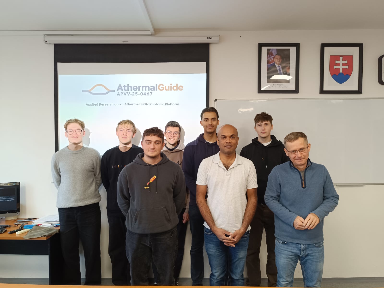
We presented AthermalGuide to students at the Slovak University of Technology in Bratislava. The project asks how an optical filter can stay tuned to a chosen wavelength as the chip temperature changes. Using a silicon oxynitride (SiON) waveguide as an example, we showed how a PMMA polymer cladding can compensate for thermal drift. For one waveguide geometry, the model predicted a shift of just 0.718 pm/°C near 1,550 nm. The team plans to test its designs by measuring photonic components at temperatures from −40 to +80 °C.

A discussion followed the presentation, covering the project’s goals and how students can take part. The closing design question gave students a concrete example: if a filter peak shifts to longer wavelengths as the chip warms up, should more or less of the guided light overlap with the polymer cladding?

Students can explore the master’s thesis topics for the 2026/2027 academic year. Another option is a paid student position developing an OFDR measurement system through the Support for Talented Students at FEI STU programme. The position pays €200 per month for up to 30 hours per month. To express your interest, contact the project lead at jozef.chovan@stuba.sk.

Send us a message

Your message will reach the project lead, who can reply to the email address you provide.

Contact

Principal investigator
Ing. Jozef Chovan, PhD.

Slovak Centre of Scientific and Technical Information
Lamačská 8A, Bratislava
jozef.chovan@cvtisr.sk
Contact form

Project funding

Slovak Research and Development Agency Agency website

Project number APVV-25-0467

Participants at the AthermalGuide presentation